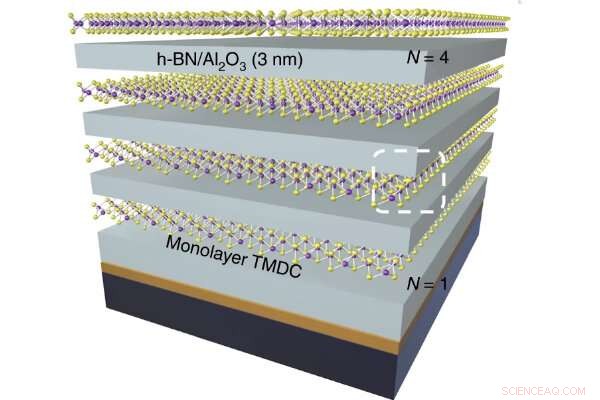
I cosiddetti materiali "bidimensionali" hanno proprietà elettriche e fotoniche uniche, ma i loro fattori di forma ultrasottili presentano sfide pratiche quando incorporati nei dispositivi. I ricercatori della Penn Engineering hanno ora dimostrato un metodo per creare "superreticoli" di grandi dimensioni - strutture a strati contenenti reticoli 2D di zolfo e tungsteno - che possono ottenere l'accoppiamento luce-materia. Credito:Università della Pennsylvania
Pannelli solari, telecamere, biosensori e fibre ottiche sono tecnologie che si basano su fotorilevatori o sensori che convertono la luce in elettricità. I fotorilevatori stanno diventando più efficienti e convenienti, con i loro chip semiconduttori componenti che stanno diminuendo di dimensioni. Tuttavia, questa miniaturizzazione sta spingendo contro i limiti imposti dai materiali e dai metodi di produzione attuali, costringendo a compromessi tra dimensioni e prestazioni.
Ci sono molte limitazioni del tradizionale processo di produzione di chip per semiconduttori. I chip vengono creati facendo crescere il film semiconduttore sopra un wafer in modo che la struttura cristallina del film sia allineata con quella del wafer di substrato. Ciò rende difficile il trasferimento della pellicola su altri materiali di supporto, riducendone l'applicabilità.
Inoltre, l'attuale metodo di trasferimento e impilamento di questi film avviene tramite esfoliazione meccanica, un processo in cui un pezzo di nastro stacca il film semiconduttore e lo trasferisce su un nuovo substrato, strato dopo strato. Questo processo si traduce in più strati non uniformi impilati l'uno sull'altro con le imperfezioni di ogni strato accumulate nell'insieme. Questo processo influisce sulla qualità del prodotto e limita la riproducibilità e la scalabilità di questi chip.
Infine, alcuni materiali non funzionano bene come strati estremamente sottili. Il silicio rimane onnipresente come materiale preferito per i chip semiconduttori, tuttavia, più diventa sottile, peggio si comporta come struttura fotonica, rendendolo tutt'altro che ideale nei fotorivelatori. Altri materiali che si comportano meglio del silicio in quanto strati estremamente sottili richiedono ancora un certo spessore per interagire con la luce, ponendo la sfida di identificare materiali fotonici ottimali e il loro spessore critico per operare nei chip semiconduttori fotorivelatori.
La produzione di film semiconduttori fotonici uniformi, estremamente sottili e di alta qualità di materiale diverso dal silicio renderebbe i chip semiconduttori più efficienti, applicabili e scalabili.
Gli ingegneri di Penn Deep Jariwala, professore assistente in ingegneria elettrica e dei sistemi, e Pawan Kumar e Jason Lynch, un borsista post-dottorato e uno studente di dottorato nel suo laboratorio, hanno condotto uno studio pubblicato su Nature Nanotechnology che mirava a fare proprio questo. Anche Eric Stach, professore di scienza e ingegneria dei materiali, insieme al suo post-dottorato Surendra Anantharaman, al dottorando Huiqin Zhang e allo studente universitario Francisco Barrera hanno contribuito a questo lavoro. Lo studio collaborativo ha incluso anche ricercatori di Penn State, AIXTRON, UCLA, Air Force Research Lab e Brookhaven National Lab, ed è stato finanziato principalmente dall'Army Research Lab. Il loro articolo descrive un nuovo metodo di produzione di superreticoli atomicamente sottili, o film semiconduttori, che sono altamente emissivi alla luce.
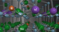
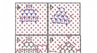
I materiali spessi un atomo generalmente assumono la forma di un reticolo, o uno strato di atomi geometricamente allineati che formano uno schema specifico per ciascun materiale. Un superreticolo è costituito da reticoli di diversi materiali impilati l'uno sull'altro. I superlattici hanno proprietà ottiche, chimiche e fisiche completamente nuove che li rendono adattabili per applicazioni specifiche come la fotoottica e altri sensori.
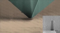
Il team di Penn Engineering ha realizzato un superreticolo, spesso cinque atomi, di tungsteno e zolfo (WS2).
"Dopo due anni di ricerca utilizzando simulazioni che ci informavano su come il superreticolo avrebbe interagito con l'ambiente, eravamo pronti per costruire sperimentalmente il superreticolo", afferma Kumar. "Because traditional superlattices are grown on a desired substrate directly, they tend to be millions of atoms thick, and difficult to transfer to other material substrates. We collaborated with industry partners to ensure that our atomically thin superlattices were grown to be scalable and applicable to many different materials."
They grew monolayers of atoms, or lattices, on a two-inch wafer and then dissolved the substrate, which allows the lattice to be transferred to any desired material, in their case, sapphire. Additionally, their lattice was created with repeating units of atoms aligned in one direction to make the superlattice two-dimensional, compact and efficient.
"Our design is scalable as well," says Lynch. "We were able to create a superlattice with a surface area measured in centimeters with our method, which is a major improvement compared to the micron scale of silicon superlattices currently being produced. This scalability is possible due to uniform thickness in our superlattices, which makes the manufacturing process simple and repeatable. Scalability is important to be able to place our superlattices on the industry-standard, four-inch chips."
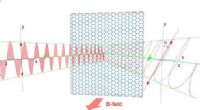
Their superlattice design is not only extremely thin, making it lightweight and cost effective, it can also emit light, not just detect it.
"We are using a new type of structure in our superlattices that involves exciton-polaritons, which are quasi-state particles made of half matter and half light," says Lynch. "Light is very hard to control, but we can control matter, and we found that by manipulating the shape of the superlattice, we could indirectly control light emitted from it. This means our superlattice can be a light source. This technology has the potential to significantly improve lidar systems in self-driving cars, facial recognition and computer vision."
Being able to both emit and detect light with the same material opens the door for more complicated applications.
"One current technology that I can see our superlattice being used for is in integrated photonic computer chips which are powered by light," says Lynch. "Light moves faster than electrons, so a chip powered by light will increase computing speed, making the process more efficient, but the challenge has been finding a light source that can power the chip. Our superlattice may be a solution there."
Applications for this new technology are diverse and will likely include high-tech robotics, rockets and lasers. Because of the wide range of applications for these superlattices, the scalability is very important.
"Our superlattices are made with a general, non-sophisticated process that does not require multiple steps in a clean room, allowing the process to be repeated easily," says Kumar. "Additionally, the design is applicable to many different types of materials, allowing for adaptability."
"In the tech world, there is a constant evolution of things moving toward the nanoscale," he says. "We will definitely be seeing a thinning down of microchips and the structures that make them, and our work in the two-dimensional material is part of this evolution."
"Of course, as we thin things down and make technology smaller and smaller, we start to interact with quantum mechanics and that's when we see interesting and unexpected phenomena occur," says Lynch. "I am very excited to be a part of a team bringing quantum mechanics into high-impact technology." + Esplora ulteriormente